WordPress Ad Banner

Microsoft Set to Unveil Its Latest AI Chip, Codenamed ‘Athena,’ Next Month

After years of development, Microsoft is on the cusp of revealing its highly-anticipated AI chip, codenamed ‘Athena,’ at the upcoming annual ‘Ignite’ event next month. This unveiling marks a significant milestone for the tech giant, as it signals a potential shift away from its reliance on GPUs manufactured by NVIDIA, the dominant player in the semiconductor industry.

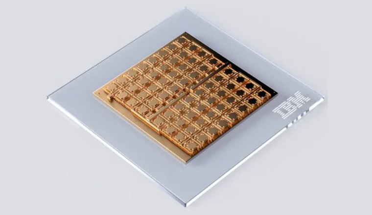
Microsoft has meticulously crafted its Athena chip to empower its data center servers, tailoring it specifically for training and running large-scale language models. The motivation behind this endeavor stems from the ever-increasing demand for NVIDIA chips to fuel AI systems. However, NVIDIA’s chips are notorious for being both scarce and expensive, with its most powerful AI offering, the H100 chip, commanding a hefty price tag of $40,000.

By venturing into in-house GPU production, Microsoft aims to curb costs and bolster its cloud computing service, Azure. Notably, Microsoft had been covertly working on Athena since 2019, coinciding with its $1 billion investment in OpenAI, the visionary organization behind ChatGPT. Over the years, Microsoft has allocated nearly $13 billion to support OpenAI, further deepening their collaboration.

Athena’s Arrival: Microsoft’s In-House AI Chip Ready for the Spotlight

Besides advancing its own AI aspirations, Microsoft’s chip could potentially aid OpenAI in addressing its own GPU requirements. OpenAI has recently expressed interest in developing its AI chip or potentially acquiring a chipmaker capable of crafting tailored chips for its unique needs.

This development holds promise for OpenAI, especially considering the colossal expenses associated with scaling ChatGPT. A Reuters report highlights that expanding ChatGPT to a tenth of Google’s search scale would necessitate an expenditure of approximately $48.1 billion for GPUs, along with an annual $16 billion investment in chips. Sam Altman, the CEO of OpenAI, has previously voiced concerns about GPU shortages affecting the functionality of his products.

To date, ChatGPT has relied on a fleet of 10,000 NVIDIA GPUs integrated into a Microsoft supercomputer. As ChatGPT transitions from being a free service to a commercial one, its demand for computational power is expected to skyrocket, requiring over 30,000 NVIDIA A100 GPUs.

Microsoft’s Athena: A Potential Game-Changer in the Semiconductor Race

The global chip supply shortage has only exacerbated the soaring prices of NVIDIA chips. In response, NVIDIA has announced the upcoming launch of the GH200 chip, featuring the same GPU as the H100 but with triple the memory capacity. Systems equipped with the GH200 are slated to debut in the second quarter of 2024.

Microsoft’s annual gathering of developers and IT professionals, ‘Ignite,’ sets the stage for this momentous revelation. The event, scheduled from November 14 to 17 in Seattle, promises to showcase vital updates across Microsoft’s product spectrum.

IBM Introduces Innovative Analog AI Chip That Works Like a Human Brain

IBM has taken the wraps off a groundbreaking analog AI chip prototype, designed to mimic the cognitive abilities of the human brain and excel at intricate computations across diverse deep neural network (DNN) tasks.

This novel chip’s potential extends beyond its capabilities. IBM asserts that this cutting-edge creation has the potential to revolutionize artificial intelligence, significantly enhancing its efficiency and diminishing the power drain it imposes on computers and smartphones.

Unveiling this technological marvel in a publication from IBM Research, the company states, “The fully integrated chip features 64 AIMC cores interconnected via an on-chip communication network. It also implements the digital activation functions and additional processing involved in individual convolutional layers and long short-term memory units.”

A Paradigm Shift in AI Computing

Fashioned within the confines of IBM Albany NanoTech Complex, this new analog AI chip comprises 64 analog in-memory compute cores. Drawing inspiration from the operational principles of neural networks within biological brains, IBM has ingeniously incorporated compact, time-based analog-to-digital converters into every tile or core. This design enables seamless transitions between the analog and digital domains.

Furthermore, each tile, or core, is equipped with lightweight digital processing units adept at executing uncomplicated nonlinear neuronal activation functions and scaling operations, as elaborated upon in an August 10 blog post by IBM.

A Potential Substitution for Existing Digital Chips

In the not-so-distant future, IBM’s prototype chip may very well take the place of the prevailing chips propelling resource-intensive AI applications in computers and mobile devices. Elucidating this perspective, the blog post continues, “A global digital processing unit is integrated into the middle of the chip that implements more complex operations that are critical for the execution of certain types of neural networks.”

As the market witnesses a surge in foundational models and generative AI tools, the efficacy and energy efficiency of conventional computing methods upon which these models rely are confronting their limits.

IBM has set its sights on bridging this gap. The company contends that many contemporary chips exhibit a segregation between their memory and processing components, consequently stymying computational speed. This dichotomy forces AI models to be stored within discrete memory locations, necessitating constant data shuffling between memory and processing units.

Drawing a parallel with traditional computers, Thanos Vasilopoulos, a researcher based at IBM’s Swiss research laboratory, underscores the potency of the human brain. He emphasizes that the human brain achieves remarkable performance while consuming minimal energy.

According to Vasilopoulos, the heightened energy efficiency of the IBM chip could usher in an era where “hefty and intricate workloads could be executed within energy-scarce or battery-constrained environments,” such as automobiles, mobile phones, and cameras.

He further envisions that cloud providers could leverage these chips to curtail energy expenditures and reduce their ecological footprint.

MIT Scientists Create More Powerful, Dense Computer Chips

The demand for more powerful, potent, and denser computer chips is constantly growing with the rise of electronic gadgets and data centers. Traditional methods for making these chips involve bulky 3D materials, which make stacking difficult. However, a team of interdisciplinary MIT researchers has developed a new technique that can grow transistors from ultrathin 2D materials directly on top of fully fabricated silicon chips.

The researchers published their findings in the peer-reviewed scientific journal Nature Nanotechnology. The new process involves growing smooth and uniform layers of 2D materials across 8-inch wafers, which can be critical for commercial applications where larger wafer sizes are typical.

The team focused on using molybdenum disulfide, a flexible and transparent 2D material with powerful electronic and photonic properties. Typically, these thin films are grown using metal-organic chemical vapor deposition (MOCVD) at temperatures above 1022 degrees Fahrenheit, which can degrade silicon circuits.

To overcome this, the researchers designed and built a new furnace with two chambers: the front, where the silicon wafer is placed in a low-temperature region, and the back, a high-temperature region. Vaporized molybdenum and sulfur compounds are then pumped into the furnace. Molybdenum stays and decomposes at the front, while the sulfur compound flows into the hotter rear and decomposes before flowing back into the front to react and grow molybdenum disulfide on the surface of the wafer.

This innovative technique is a significant advancement in the development of more powerful and denser computer chips. With this breakthrough, the researchers were able to construct multistory building-like structures, significantly increasing the density of integrated circuits. In the future, the team hopes to fine-tune their technique and explore growing 2D materials on everyday surfaces like textiles and paper, potentially revolutionizing the industry.