WordPress Ad Banner

GoChess: New Smart Robotic Chess Board

Chess enthusiasts around the globe have a reason to rejoice as electronic gaming startup Particula unveils its latest innovation – GoChess.

This groundbreaking chess set effectively bridges the gap between traditional board games and virtual gameplay by offering players the opportunity to compete in online matches with the assistance of robotic chess pieces.

GoChess, with its ability to seamlessly blend physical and virtual elements, is poised to transform the way chess is played, offering players of all skill levels an engaging and dynamic experience. The project has already gained significant traction through a highly successful Kickstarter campaign that is currently underway.

Fusion of Physical and Virtual Gameplay

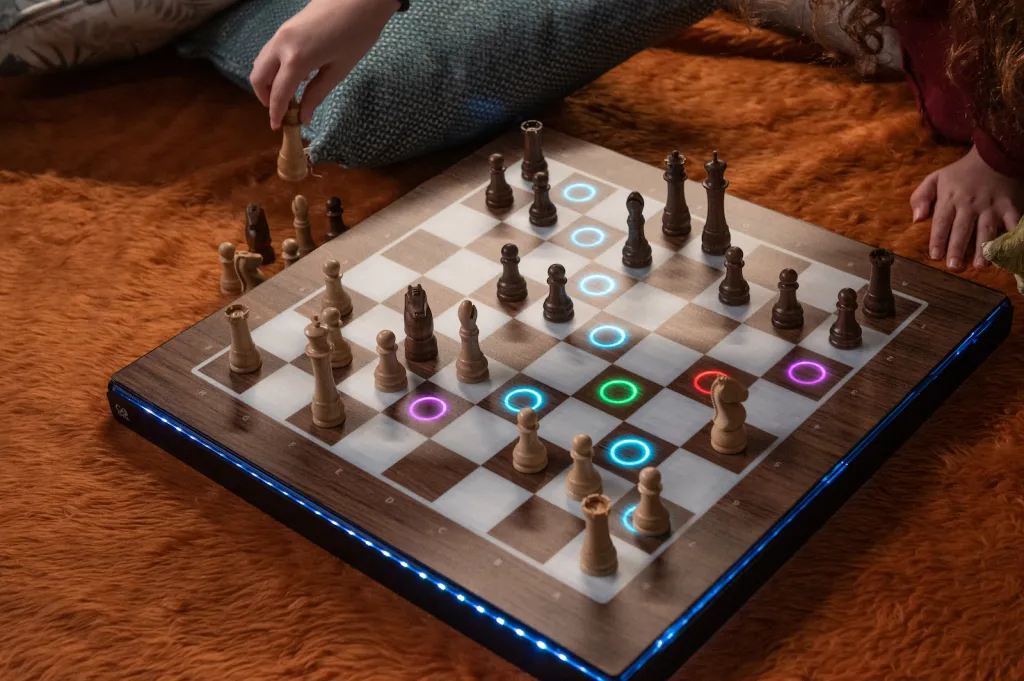
The perfect fusion of physical and virtual gameplay, GoChess appears at first glance to be a conventional chess set. The magnetic chess pieces glide effortlessly across the board, facilitated by a network of miniature wheeled robots cleverly concealed beneath the translucent surface.

GoChess syncs with online chess venues like Lichness and Chess.com through a Bluetooth connection to a companion app, enabling players to face off against opponents who are far away in real-time. 

GoChess uses sensors to detect and record moves made on its physical board while players can make moves using their computer keyboards or on-screen chess boards.

A variety of features are available in GoChess that are intended to improve the chess playing experience. Users can test an online AI opponent against them at various levels of difficulty, which enables gamers to constantly advance their abilities. 

Each square has coloured LEDs underneath it that offer coaching by proposing possible actions and providing advice on wise and foolish decisions. Additionally, the companion app enables lone players to solve brainteasers and even watch well-known historical chess tournaments. The software also functions as a thorough game tracker, keeping track of advancement and offering tailored suggestions for better gameplay.

smart robotic chess board

GoChess’ portable design meets the needs of chess enthusiasts who are constantly on the move. Players can enjoy a game of chess anywhere thanks to the board’s detachable, independently usable sensor and LED surface. 

GoChess Lite, which offers standalone chessboard capability without the robotic capabilities, is an alternative for people on a tight budget. GoChess also supports traditional face-to-face gameplay, giving players who prefer the time-honored custom of manually moving their pieces a flexible solution.

Affordable pricing and future prospects

The GoChess Lite option costs $219, while pledges for the complete GoChess system start at $259 per. 

In comparison to the anticipated retail prices of $379 and $319, respectively, these figures represent significant savings. If everything goes as planned, backers can anticipate receiving their boards by May 2024. 

Alternatives for chess players looking for similar advances include the SquareOff and Phantom robotic chess boards, each of which offers special features that suit individual interests.

GoChess ushers in a new era of chess by fusing its age-old allure with the practicality and opportunities of the digital world. GoChess delivers a singular experience that will enthrall chess enthusiasts all over the world, whether players are looking for competitive online matches, want to improve their skills, or simply enjoy a typical chess game.

Bill Gates-Backed Company, CubicPV, Advances Perovskite Solar Panels for Commercialization

CubicPV, a company supported by Bill Gates’ Breakthrough Energy Ventures, is working towards commercializing perovskite panels to significantly enhance the viability of solar energy. Based in Massachusetts and Texas, the firm is engineering innovative solar panels featuring a bottom silicon layer and a top perovskite layer, resulting in an impressive efficiency rate of 30 percent.

A recent report by CNBC highlighted CubicPV’s progress in this field. CEO Frank van Mierlo shared with the news outlet that the company’s perovskite chemistry and cost-effective manufacturing method for the silicon layer make their products economically attractive.

The company’s efforts have not gone unnoticed. Last month, the Department of Energy announced CubicPV as the lead industry participant in a new research center at the Massachusetts Institute of Technology. Together, these organizations will leverage automation and artificial intelligence to significantly enhance the production and development of tandem panels.

“Tandem extracts more power from the sun, making every solar installation more powerful and accelerating the world’s ability to curb the worst impacts of climate change,” explained Van Mierlo in the CNBC interview. He further expressed his belief that the entire solar industry will transition to tandem panels within the next decade.

Additionally, CubicPV is actively searching for a suitable location in the United States to construct a new 10GW silicon wafer plant. This step signifies the company’s commitment to expanding its production capacity and contributing to the growth of the solar energy sector.

With the support of Bill Gates and ongoing technological advancements, CubicPV is making significant strides in the development of perovskite solar panels, offering a promising solution for a cleaner and more sustainable future.

Challenges ahead

But all is not rosy yet! Perovskites still face many hurdles in terms of cost and durability. 

Lead halide perovskites are winning the race to be the best performing so far but researchers are still trying to formulate other compositions to avoid lead toxicity.

Martin Green, who heads the Australian Centre for Advanced Photovoltaics, told CNBC that silicon-based tandem cells are likely to be the next big development in solar technology even though they currently do not work well enough outside the lab.

“The big question is whether perovskite/silicon tandem cells will ever have the stability required to be commercially viable,” told CNBC Green.

“Although progress has been made since the first perovskite cells were reported, the only published field data for such tandem cells with competitive efficiency suggest they would only survive a few months outdoors even when carefully encapsulated.”

Will CubicPV be able to bypass this challenge and produce the tech the nation so desperately needs to make solar more viable and productive? Only time will tell.

Empowering an AI-First Future: Meta Unveils New AI Data Centers and Supercomputer

Meta, formerly known as Facebook, has been at the forefront of artificial intelligence (AI) for over a decade, utilizing it to power their range of products and services, including News Feed, Facebook Ads, Messenger, and virtual reality. With the increasing demand for more advanced and scalable AI solutions, Meta recognizes the need for innovative and efficient AI infrastructure.

At the recent AI Infra @ Scale event, a virtual conference organized by Meta’s engineering and infrastructure teams, the company made several announcements regarding new hardware and software projects aimed at supporting the next generation of AI applications. The event featured Meta speakers who shared their valuable insights and experiences in building and deploying large-scale AI systems.

One significant announcement was the introduction of a new AI data center design optimized for both AI training and inference, the primary stages of developing and running AI models. These data centers will leverage Meta’s own silicon called the Meta training and inference accelerator (MTIA), a chip specifically designed to accelerate AI workloads across diverse domains, including computer vision, natural language processing, and recommendation systems.

Meta also unveiled the Research Supercluster (RSC), an AI supercomputer that integrates a staggering 16,000 GPUs. This supercomputer has been instrumental in training large language models (LLMs), such as the LLaMA project, which Meta had previously announced in February.

“We have been tirelessly building advanced AI infrastructure for years, and this ongoing work represents our commitment to enabling further advancements and more effective utilization of this technology across all aspects of our operations,” stated Meta CEO Mark Zuckerberg.

Meta’s dedication to advancing AI infrastructure demonstrates their long-term vision for utilizing cutting-edge technology and enhancing the application of AI in their products and services. As the demand for AI continues to evolve, Meta remains at the forefront, driving innovation and pushing the boundaries of what is possible in the field of artificial intelligence.

Building AI infrastructure is table stakes in 2023

Meta is far from being the only hyperscaler or large IT vendor that is thinking about purpose-built AI infrastructure. In November, Microsoft and Nvidia announced a partnership for an AI supercomputer in the cloud. The system benefits (not surprisingly) from Nvidia GPUs, connected with Nvidia’s Quantum 2 InfiniBand networking technology.

A few months later in February, IBM outlined details of its AI supercomputer, codenamed Vela. IBM’s system is using x86 silicon, alongside Nvidia GPUs and ethernet-based networking. Each node in the Vela system is packed with eight 80GB A100 GPUs. IBM’s goal is to build out new foundation models that can help serve enterprise AI needs.

Not to be outdone, Google has also jumped into the AI supercomputer race with an announcement on May 10. The Google system is using Nvidia GPUs along with custom designed infrastructure processing units (IPUs) to enable rapid data flow. 

What Meta’s new AI inference accelerator brings to the table

Meta is now also jumping into the custom silicon space with its MTIA chip. Custom built AI inference chips are also not a new thing either. Google has been building out its tensor processing unit (TPU) for several years and Amazon has had its own AWS inferentia chips since 2018.

For Meta, the need for AI inference spans multiple aspects of its operations for its social media sites, including news feeds, ranking, content understanding and recommendations. In a video outlining the MTIA silicon, Meta research scientist for infrastructure Amin Firoozshahian commented that traditional CPUs are not designed to handle the inference demands from the applications that Meta runs. That’s why the company decided to build its own custom silicon.

“MTIA is a chip that is optimized for the workloads we care about and tailored specifically for those needs,” Firoozshahian said.

Meta is also a big user of the open source PyTorch machine learning (ML) framework, which it originally created. Since 2022, PyTorch has been under the governance of the Linux Foundation’s PyTorch Foundation effort. Part of the goal with MTIA is to have highly optimized silicon for running PyTorch workloads at Meta’s large scale.

The MTIA silicon is a 7nm (nanometer) process design and can provide up to 102.4 TOPS (Trillion Operations per Second). The MTIA is part of a highly integrated approach within Meta to optimize AI operations, including networking, data center optimization and power utilization.

Meet Apple’s M3 Chipset: A 12-Core CPU and 18-Core GPU Monster

According to various news outlets, like Bloomberg, Apple is currently testing its latest chipset, the M3. The new chipset, it is claimed, will come with a mighty 12-core processor and 18-core graphical processing unit (GPU). Bloomberg claims they came across this information from the reporter’s receipt of an App Store developer log showing the chip running on an unannounced MacBook Pro with macOS 14.

If true, Bloomberg speculates that the new M3 chip is likely the base-level M3 Pro that Apple plans to release sometime in 2024. This is interesting as Apple is about to introduce its new M2 Macs. Apple’s latest silicon technology, the M2 chip, boasts improved speed and power efficiency compared to its predecessor, the M1 chip.

The 8-core CPU offers increased processing power, enabling faster task completion. The 10-core GPU is ideal for creating stunning images and animations. Moreover, users can work with multiple 4K and 8K ProRes video streams thanks to the powerful media engine. The cherry on top, according to Apple, is the impressive battery life of up to 18 hours, allowing users to work or play uninterrupted throughout the day.

The M3 series is anticipated to benefit from Taiwan Semiconductor Manufacturing Company’s (TSMC’s) upcoming 3nm node process. The decrease in core density would be caused by the switch from 5nm to 3nm. Recall that the M1 Pro and M2 Pro have 14 and 16-core GPUs and eight and 10-core processors.

In other words, the M3 Pro is said to have 50 percent more CPU cores than its first-generation forerunner. Bloomberg also claims that Apple chose to have an equal number of high-performance and efficient cores on the new silicon. He claims that the chip was discovered with 36 GB of RAM installed. To put things in perspective, the M2 Pro comes standard with 16 GB of memory, but you can upgrade it to 32 GB.

Naturally, Apple must release the M3 processor in its standard form before announcing the M3 Pro. According to Bloomberg‘s report, “the first Macs with M3 chips will start showing up toward the end of the year or early next year.” The long-rumored 15-inch MacBook Air is anticipated to be unveiled by Apple at WWDC 2023 in the interim.

Quantum Computer Creates Particle That Can Remember Its Past

In a significant advancement for quantum computing, a recent report by New Scientist reveals that a quantum computer has successfully generated a particle known as an anyon, which possesses the ability to retain its past states. This groundbreaking development carries the potential to enhance the capabilities of quantum computing systems.

Unlike conventional particles, anyons possess a unique characteristic of maintaining a form of memory concerning their previous locations. Initially observed in the 1970s, anyons exist solely in two dimensions and exhibit quasiparticle properties—collective vibrations that exhibit particle-like behavior.

Of particular interest are the so-called swapping anyons, which retain a record of the number of swaps they undergo, influencing their vibrational patterns. This intriguing quality makes them a compelling avenue for quantum computing. However, until now, experimental confirmation of their existence had remained elusive.

Enter Henrik Dryer and his team at the quantum computing company Quantinuum. They have made a remarkable breakthrough with the development of a cutting-edge quantum processor called H2. This quantum processor has the capability to generate qubits, the fundamental units of quantum information, and also introduce surface anyons—a significant achievement in the field.

With this advancement, the potential for leveraging anyons in quantum computing systems takes a significant leap forward. The ability of anyons to retain and manipulate information from previous states holds tremendous promise for enhancing the computational power and efficiency of future quantum computers.

A Kagome Lattice

They did this by entangling these qubits in a formation called a Kagome lattice, a pattern of interlocking stars common in traditional woven Japanese baskets, giving them identical quantum mechanical properties to those predicted for anyons.

“This is the first convincing test that’s been able to do that, so this would be the first case of what you would call non-Abelian topological order,” told New Scientist Steven Simon at the University of Oxford. 

Enhancing Battery Life for IoT Devices: MIT’s Terahertz Wake-Up Receiver Chip

An ultra-compact terahertz wake-up receiver chip has been created by MIT engineers that uses only a few microwatts of power and comes with a low-power authentication system to defend against denial-of-sleep assaults. Wake-up receivers have grown more important as smaller Internet of Things (IoT) devices have gained popularity. 

Eunseok Lee, a graduate student in MIT’s Electrical Engineering and Computer Science Department, said, “If it is turned on constantly, it will consume a whole lot of power, right? So what a wake-up receiver does is keep an electronic device at a very low power mode [until] we send a signal to the receiver so that it can activate the entire system.”

“By using terahertz frequencies, we can make an antenna that is only a few hundred micrometers on each side, which is a very small size. This means we can integrate these antennas to the chip, creating a fully integrated solution. Ultimately, this enabled us to build a very small wake-up receiver that could be attached to tiny sensors or radios,” he added further. 

Reduced antenna size and increased security of terahertz waves

Most common wake-up receivers currently in use employ Wi-Fi or Bluetooth, with frequencies around 2.4 GHz and wavelengths of about 12.5 centimeters, necessitating the use of centimeter-scale receivers. The MIT researchers’ receiver is substantially smaller since it was designed to transmit at terahertz frequencies, equivalent to wavelengths between 1 and 0.03 millimeters. In addition to being more secure than radio waves, terahertz waves are also much less mobile due to their high frequencies.

The researchers blended two terahertz frequencies using two small transistors as antennas for its detector at a low power cost, leveraging terahertz self-mixing to prevent the large power consumption brought on by mixing with another signal. To guard against denial-of-sleep assaults, in which an attacker tries to activate the gadget repeatedly in an effort to drain its battery, they also installed a wake-up authentication circuit within their terahertz receiver.

Potential applications

There are many potential uses for the tiny terahertz wake-up receiver, including putting it inside microbots that watch over spaces too small or unsafe for humans, using the sensors in unobtrusive indoor security applications, and using robot swarms to gather localized data. The team is constructing a platform for terahertz wave harvesting. Lee also mentioned that they are enhancing the wake-up receiver’s angular sensitivity and wish to optimize terahertz technologies for practical applications.

World’s Smallest LED Will Convert Your Phone Camera into a Microscope

A research team from Singapore-MIT Alliance for Research and Technology (SMART) has created a silicon LED capable of transforming the camera on a mobile phone into a high-resolution microscope. This LED delivers a light intensity similar to larger silicon LEDs and was used to develop the world’s smallest holographic microscope, which has various potential applications.

The team also devised a neural networking algorithm to reconstruct objects captured by the holographic microscope. These networks, based on the signaling between neurons in the human brain, are a form of machine learning. This development removes the need for traditional, bulky microscopes, making it possible for their all-in-one chip to examine microscopic objects like microorganisms and tissue cells.

Successfully solving a challenge

The innovation paves the way for advancement in photonics – an area of technology that deals with studying and technological harnessing of light. The press release says that the building of a powerful on-chip emitter that is smaller than a micrometer has long been a challenge in the field, which the research team has had a breakthrough in.

Previously, scientists have struggled to place such on-chip emitters into standard complementary metal-oxide-semiconductor (CMOS) platforms, which is the semiconductor technology used in most chips today. In mobile phones, CMOS is used as the ‘eye’ of the camera.

The researchers think that this combination of CMOS micro-LEDs and their newly developed neural network can be applied in other areas as well, such as live-cell tracking or spectroscopic imaging of biological tissues.

“On top of its immense potential in lensless holography, our new LED has a wide range of other possible applications. Because its wavelength is within the minimum absorption window of biological tissues, together with its high intensity and nanoscale emission area, our LED could be ideal for bio-imaging and bio-sensing applications, including near-field microscopy and implantable CMOS devices,” said Rajeev Ram, a co-author of the paper. “Also, it is possible to integrate this LED with on-chip photodetectors, and it could then find further applications in on-chip communication, NIR proximity sensing, and on-wafer testing of photonics.”

Established in 2007, SMART was set up in collaboration with the Massachusetts Institute of Technology in Cambridge and is its largest international research endeavor.

MIT Scientists Create More Powerful, Dense Computer Chips

The demand for more powerful, potent, and denser computer chips is constantly growing with the rise of electronic gadgets and data centers. Traditional methods for making these chips involve bulky 3D materials, which make stacking difficult. However, a team of interdisciplinary MIT researchers has developed a new technique that can grow transistors from ultrathin 2D materials directly on top of fully fabricated silicon chips.

The researchers published their findings in the peer-reviewed scientific journal Nature Nanotechnology. The new process involves growing smooth and uniform layers of 2D materials across 8-inch wafers, which can be critical for commercial applications where larger wafer sizes are typical.

The team focused on using molybdenum disulfide, a flexible and transparent 2D material with powerful electronic and photonic properties. Typically, these thin films are grown using metal-organic chemical vapor deposition (MOCVD) at temperatures above 1022 degrees Fahrenheit, which can degrade silicon circuits.

To overcome this, the researchers designed and built a new furnace with two chambers: the front, where the silicon wafer is placed in a low-temperature region, and the back, a high-temperature region. Vaporized molybdenum and sulfur compounds are then pumped into the furnace. Molybdenum stays and decomposes at the front, while the sulfur compound flows into the hotter rear and decomposes before flowing back into the front to react and grow molybdenum disulfide on the surface of the wafer.

This innovative technique is a significant advancement in the development of more powerful and denser computer chips. With this breakthrough, the researchers were able to construct multistory building-like structures, significantly increasing the density of integrated circuits. In the future, the team hopes to fine-tune their technique and explore growing 2D materials on everyday surfaces like textiles and paper, potentially revolutionizing the industry.

The World’s First Electrical Wooden Transistor Has Finally Been Invented

Researchers at Linköping University and the KTH Royal Institute of Technology have achieved a major breakthrough in the field of efficiency and sustainability with the creation of the world’s first wooden electrical transistor.

According to a press release by the institutions, the team developed an unprecedented principle that enables the transistor to function continuously and regulate electricity flow without deteriorating. The transistor was created using balsa wood, which is a grainless wood that is evenly structured throughout and was filled with a conductive polymer called PEDOT:PSS. This resulted in an electrically conductive wood material that can regulate electricity flow without issues.

Previous attempts at creating wooden transistors only succeeded in regulating ion transport, but this new development has the potential for huge advancements. Isak Engquist, senior associate professor at the Laboratory for Organic Electronics at Linköping University, noted that although the wood transistor is currently slow and bulky, it has significant potential for development.

The researchers achieved this success by removing lignin from the wood, leaving only long cellulose fibers with channels where the lignin had been. The channels were then filled with the conductive polymer to create the new device. With this development, the scientific community has made significant strides in the field of sustainability, creating a more environmentally-friendly option for electronic devices.

Switching the power on and off

These changes led to a wood transistor that is able to regulate electric current and provide continuous function at a selected output level. Better yet, it could even switch the power on and off with an almost insignificant delay.

Switching it off takes about a second while turning it on takes about five seconds.

The final transistor channel is quite large but the researchers stated that this is a benefit as it could potentially tolerate a higher current than regular organic transistors, which could be important for certain future applications. 

“We didn’t create the wood transistor with any specific application in mind. We did it because we could. This is basic research, showing that it’s possible, and we hope it will inspire further research that can lead to applications in the future,” concluded Isak Engquist in the statement.

World’s First Triple Optical Camera Drone Offers Advanced Imaging Capabilities

Pushing the realms of next-level imaging performance concerning drone cameras, DJI has released a novel triple-camera setup with its Mavic 3 Pro, equipped with a Hasselblad camera and dual telephoto lenses.

The flagship drone’s triple camera combination lets content creators switch between shot compositions with just one tap, resulting in a wider variety of shots in less time. Lenses with multiple focal lengths (24mm/70mm/166mm) provide multi-scenario capabilities, be it capturing the “environment with the wide-angle, moving into a specific location with the medium tele and then focusing on a particular area or character,” said a blog post

Advanced Hasselblad camera offers rich images

The 4/3 CMOS Hasselblad camera on offer with the Mavic 3 Pro supports shooting 12-bit RAW photos with a “native dynamic range” and efficient post-production without losing image quality or clarity.

Professional creators can make use of Mavic 3 Pro’s cameras that support Apple ProRes 422 HQ, Apple ProRes 422, and App dynamic range of up to 12.8 stops. Additionally, the Hasselblad Natural Colour Solution (HNCS) enables it to process colors organically, eliminating the need for heavy post-production or complex color presets. The primary lens also offers professional video specifications with image capture supported up to 5.1K at 50fps or DCI 4K at 120fps. The new 10-bit D-Log M color mode offered by DJI supports recording up to one billion colors, ensuring “natural color gradations with delicate details for a full-spectrum visual experience.” A 1TB SSD and a 10Gbps lightspeed data cable also help to smoothen the processing and editing of images.

Telelenses offer advanced subject framing and zoom capabilities

The medium tele camera suits various themes and scenes. The 1/1.3″ CMOS sensor offers 3x optical zoom and is capable of generating 48MP/12MP photos, 4K/60fps video, and supports the new D-log M. The camera ensures that creators can produce the perfect Hyperlapse videos. 

The upgraded tele camera on the Mavic 3 Pro features higher resolution and a wider f/3.4 aperture. “It supports shooting 4K/60fps video with 7x optical zoom and 12MP photos.” With a hybrid zoom of up to 28x, the drone can safely keep a good distance from its subject and still capture rich images. 

Extended range and safety on offer

The new iteration from DJI now offers 43 minutes of flight time, letting users explore and experiment with their work, from flight route planning to shot composition, all during a single flight.

In terms of advanced safety while in motion, eight wide-angle vision sensors feed data to a high-performance vision computing engine to “precisely sense obstacles in all directions and plan a safe flight route to avoid them.” 

A signal transmission distance of up to 15 km is supported by the Mavic 3 Pro, and it can transmit a 1080p/60fps HD live feed, making it more responsive and providing a vibrant video feed onto the monitor.